- 您现在的位置:买卖IC网 > Sheet目录541 > ZXMP6A18KTC (Diodes Inc)MOSFET P-CHAN 60V DPAK
ZXMP6A18K
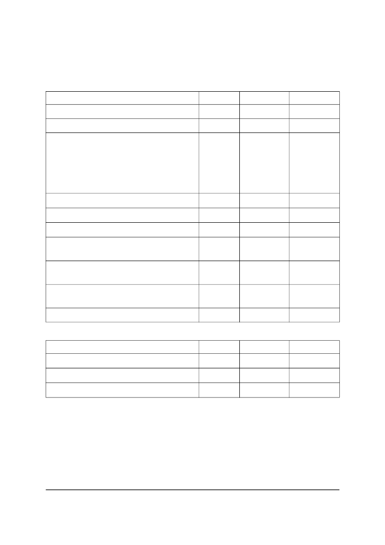
Absolute maximum ratings
Parameter
Drain-source voltage
Gate-source voltage
Symbol
V DSS
V GS
Limit
-60
±20
Unit
V
V
Continuous drain current
@V GS =10V; T A =25°C (b)
-10.4
A
@V GS =10V; T A =70°C (b)
@V GS =10V; T A =25°C (a)
Pulsed drain current (c)
Continuous source current (body diode) (b)
Pulsed source current (body diode) (c)
Power dissipation at T A =25°C (a)
Linear derating factor
Power dissipation at T A =25°C (b)
Linear derating factor
Power dissipation at T A =25°C (d)
Linear derating factor
Operating and storage temperature range
I D
I DM
I S
I SM
P D
P D
P D
T j :T stg
-8.3
-6.8
-37.5
-11.5
-37.5
4.3
34.4
10.1
80.8
2.15
17.2
-55 to +150
A
A
A
A
A
W
mW/°C
W
mW/°C
W
mW/°C
°C
Thermal resistance
Parameter
Junction to ambient (a)
Junction to ambient (b)
Junction to ambient (d)
Symbol
R JA
R JA
R JA
Value
29
12.3
58
Unit
°C/W
°C/W
°C/W
NOTES:
(a) For a device surface mounted on 50mm x 50mm x 1.6mm FR4 PCB with high coverage of single sided 2oz copper, in
still air conditions.
(b) For a device surface mounted on FR4 PCB measured at t 10 sec.
(c) Repetitive rating 50mm x 50mm x 1.6mm FR4 PCB, D=0.02 pulse width=300 s - pulse width limited by maximum
junction temperature.
(d) For a device surface mounted on 25mm x 25mm x 1.6mm FR4 PCB with high coverage of single sided 1oz copper, in
still air conditions.
Issue 1 - March 2006
? Zetex Semiconductors plc 2006
2
www.zetex.com
发布紧急采购,3分钟左右您将得到回复。
相关PDF资料
ZXMP7A17GTA
MOSFET P-CH 70V 3.7A SOT-223
ZXMP7A17KTC
MOSFET P-CH 70V 5.7A D PAK
1-46673-0
TOOL HEAD CRIMP 22-16AWG STRATO
1-47387-0
TOOL HEAD CRIMP 16-14AWG PIDG
1-49935-0
TOOL HEAD CRIMP 22-10AWG SOLIS
0010844061
084 DIA ASSY HDR HSG PIN 94V-0
0011020001
INSERTION TOOL HT1807
0011020003
INSERTION TOOL HT1353
相关代理商/技术参数
ZXMP7A17G
制造商:Diodes Incorporated 功能描述:MOSFET P SOT-223 制造商:Diodes Incorporated 功能描述:MOSFET, P, SOT-223 制造商:DIODES 功能描述:MOSFET, P, SOT-223, Transistor Polarity:P Channel, Continuous Drain Current Id:3 制造商:Diodes Incorporated 功能描述:MOSFET, P CH, 70V, -3.7A, SOT-223, Transistor Polarity:P Channel, Continuous Drain Current Id:-3.7A, Drain Source Voltage Vds:70V, On Resistance Rds(on):160mohm, Rds(on) Test Voltage Vgs:10V, Threshold Voltage Vgs:-1V, No. of Pins:4 , RoHS Compliant: Yes
ZXMP7A17GTA
功能描述:MOSFET P-Ch 70V 3.7A RoHS:否 制造商:STMicroelectronics 晶体管极性:N-Channel 汲极/源极击穿电压:650 V 闸/源击穿电压:25 V 漏极连续电流:130 A 电阻汲极/源极 RDS(导通):0.014 Ohms 配置:Single 最大工作温度: 安装风格:Through Hole 封装 / 箱体:Max247 封装:Tube
ZXMP7A17GTC
制造商:DIODES 制造商全称:Diodes Incorporated 功能描述:70V P-channel enhancement mode MOSFET
ZXMP7A17K
制造商:DIODES 制造商全称:Diodes Incorporated 功能描述:70V P-channel enhancement mode MOSFET
ZXMP7A17KTC
功能描述:MOSFET 70V P-Channel 5.7A MOSFET RoHS:否 制造商:STMicroelectronics 晶体管极性:N-Channel 汲极/源极击穿电压:650 V 闸/源击穿电压:25 V 漏极连续电流:130 A 电阻汲极/源极 RDS(导通):0.014 Ohms 配置:Single 最大工作温度: 安装风格:Through Hole 封装 / 箱体:Max247 封装:Tube
ZXMS6001
制造商:ZETEX 制造商全称:ZETEX 功能描述:60V N-channel self protected enhancement mode INTELLIFETTM MOSFET
ZXMS6001N3
制造商:ZETEX 制造商全称:ZETEX 功能描述:60V N-channel self protected enhancement mode INTELLIFETTM MOSFET
ZXMS6001N3TA
功能描述:电源开关 IC - 配电 60V LO INPT CURR SELF PROT LO SD SWCH RoHS:否 制造商:Exar 输出端数量:1 开启电阻(最大值):85 mOhms 开启时间(最大值):400 us 关闭时间(最大值):20 us 工作电源电压:3.2 V to 6.5 V 电源电流(最大值): 最大工作温度:+ 85 C 安装风格:SMD/SMT 封装 / 箱体:SOT-23-5
